Control Panel: Difference between revisions
From Star Trek: Theurgy Wiki
Auctor Lucan (talk | contribs) (Created page with "right|400pxControlled/display surfaces were composed of three basic layers. The outermost layer was fabricated from a 2.5 mm tripolymer-coated tran...") |
Auctor Lucan (talk | contribs) No edit summary |
||
| Line 5: | Line 5: | ||
The substrate of the controlled surface was composed of microfoamed polyduranide sheeting, which provided structural integrity to the assembly. Incorporated into this layer was a matrix of optical nanoprocessors that permitted the display surface sheeting to be self-configuring, once addressed and initialized by the local processor node. For redundancy's sake, the panel nanoprocessors included sufficient nonvolatile memory to permit system operation, even in the absence of main computer support. | The substrate of the controlled surface was composed of microfoamed polyduranide sheeting, which provided structural integrity to the assembly. Incorporated into this layer was a matrix of optical nanoprocessors that permitted the display surface sheeting to be self-configuring, once addressed and initialized by the local processor node. For redundancy's sake, the panel nanoprocessors included sufficient nonvolatile memory to permit system operation, even in the absence of main computer support. | ||
====Disclaimer==== | |||
''Image and text from the [[Starfleet]] Technical Manual.'' | |||
[[Category:General Information]][[Category:Starfleet Information]][[Category:Equipment]] | [[Category:General Information]][[Category:Starfleet Information]][[Category:Equipment]] | ||
Latest revision as of 22:00, 1 October 2019
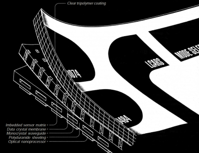
Controlled/display surfaces were composed of three basic layers. The outermost layer was fabricated from a 2.5 mm tripolymer-coated transparent aluminium wafer into which was embedded a sensor matrix. This matrix detected tactile input by the operator's fingertips. Also incorporated into this layer was a transducer matrix that provides tactile and auditory feedback to the operator, indicating that a particular controlled surface addressed had been activated.
The aluminium surface wafer was chemically bond onto a triaxial optical display crystal membrane, which served as a high resolution graphic display medium. Monocrystal microwaveguides at 1. 8 mm intervals provided electro plasma system power transmission to the upper sensor matrix and transducer layers.
The substrate of the controlled surface was composed of microfoamed polyduranide sheeting, which provided structural integrity to the assembly. Incorporated into this layer was a matrix of optical nanoprocessors that permitted the display surface sheeting to be self-configuring, once addressed and initialized by the local processor node. For redundancy's sake, the panel nanoprocessors included sufficient nonvolatile memory to permit system operation, even in the absence of main computer support.
Disclaimer
Image and text from the Starfleet Technical Manual.

